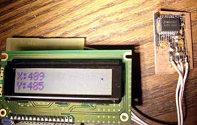
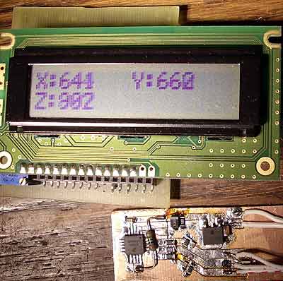
Next toys connected to my AVR-USB testing board are two Freescale semiconductors (ex Motorola) accelerometer chips: MMA3202D and MMA7260QT. First is “catastrophic” accelerometer chip with high-G (100g X-axis and 50g Y-axis) sensor. If you apply such acceleration to human body it will squash to yogurt. Bet in real world such forces are achieved in various accidents- just drop down your hard disk to stone floor and the force will be about this. 🙂 Sensitivity is not very high, but it is possible to detect static gravity force or free fall.

Next chip is more sensitive, so called low-G sensor. (Selectable Sensitivity (1.5g/2g/4g/6g)). It has 3 axis. As this device required 3.3V power supply, I placed small linear regulator on board. All other stuff on PCB is to filter electric noise. The device is very noisy. First I thought that my PCB and AVR analog input is the source of the noise, but after visiting Freescale seminar and looking at original demo board of the same chip I found that the chip itself is very noisy.

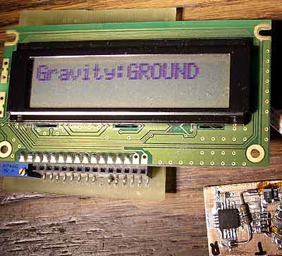
There is small example in software to demonstrate the usage of the chip. When jumper “firmaware” in ON, the LCD display is showing the position of sensor PCB. It is useful to use such feature in video and photo cameras to display pictures in LCD display. Or to reduce handshaking. I didn’t implemented “free fall” feature in my source. But is very easy to do- just detect 0g on all three axis. It is useful to use 0g detection in some notebook computers or hard disks. Just to park shock sensitive devices and prevent them from shock damage. Another interesting device is small shock logger- just to collect data in some parcel. But there is bad side from this technology. In near future, all handheld devices will have such loggers. And if your device will fall down to ground it will log this accident. And in local repair shop, your device will betray you. 🙂

The software is very simple. All freescale chips are analog chips. I was asking about I2C or other chips (they are promoted in website), but freescale representative was very mysterious about the developing schedule. So now I just measure the output with ADC converter and interpret the answers.
Source code: 20071102.zip.
There is NO PCB for these devices. My laserjet printer is bad and PCB are very simple. So I hand cut the traced with small graver. Even for leadless QFN chip.
