
Tools:
- Soldering iron, with thermal control preferred.
- Tweezers.
- Side Cutters.
- Hot air soldering station – optional, but it makes life easy.
- Leaded solder with flux core. Some flux.
- Some PCB cleaning fluid, alcohol, Contact cleaner.
- Multi-meter.
- Oscilloscope 🙂 – in case you want see everything by your self.
Not all components are needed to start a project. Not all tools are mandatory. There are no strict rules about building this project, but this manual will help you to build it without big problems.
First of all- inspect the PCB for damage or shorts. Typically, visual inspection is enough, but I always check 5V lines for short to GND planes. I also refresh all the SMD solder pads on the PCB. Original “china” tin plating sometimes is very hard to solder.
Step 1:
Start by building this part of the circuit:
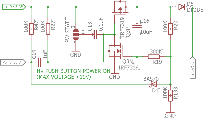
This part of the circuit may change in the next revision because I don’t like how it works. The double FET is in the SOIC8 package, and almost any transistor can be placed here. The only important thing- maximum gate voltage (limits max input voltage) and package. Solder nice red LED (“+19V”) and R41 resistor (about 5K6, depending on the brightness of your LED and input voltage).
When this part is completed, and the power-in jack (J5) soldered, connect the board to limited power supply. Short connection of power control header (J9, pin 1) to ground (pin 2 or any other GND) must connect external power to C18 positive terminal. Long connection of pin 1 must switch off power.
Step 2:
Building 5V power regulator.
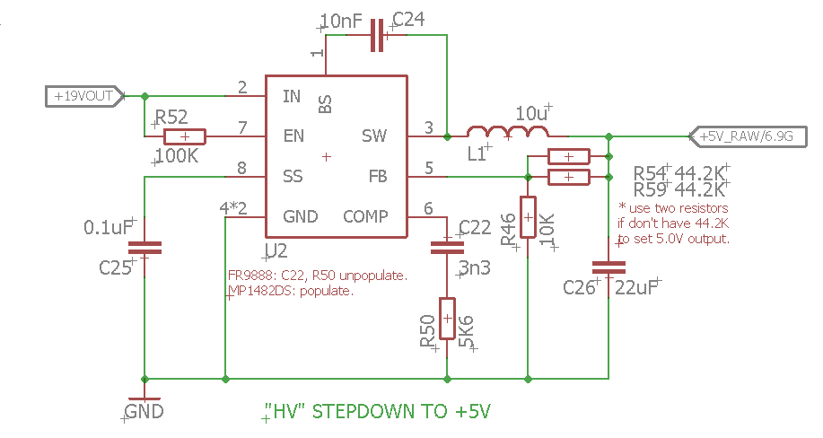
Acquire U2 chip from any source (Aliexpress, salvage from PCIe risers used in mining farms or buy something from an expensive dealer). The PCB can accept FR9888 chip (or some other from this family) or MP1428DS (or some from this family), (untested: AN6484, 24V in, 3A out; MP2307). I think there are also some brand chips with the same pin-out. When using RF9888, do not populate C22 and R50- this is not used in this chip.
SMD inductor for FR9888 is 10uH and up to 3A current, lots of reserved power. In the next version of PCB I’ll make it possible to use smaller inductors.
To select output voltage, R46 must be 10K and resistance in R54/R59 must be 44.2K. It is a rare resistor, so that’s why I put two resistors in parallel (R54 and R59). Combining 56K and 220K resistors here and 10K resistor R46 gives me 5.06V output.
Temporary solder ~0.2 ohm or a bit bigger resistor instead of L2. This will protect custom Atari chips in case of emergency. The step-down power converter has enough juice to fry any chip without problem.
Jumper near C30, market “DANGER!” bypass 5V regulator. When powering from 5V internal or external power supply, do not populate 5V voltage regulator and close this jumper. When powering from “high voltage” PSU, “high” voltage is “near” 5V bus. Do not close this jumper. It is made wide and SMD just to prevent accidental shorts.
Check voltage on TTL chip pads.
For FR9888 there is no need for electrolytic caps. Those big SMD caps are salvaged from some computer or VGA boards. About 10 or 25µF each, was on 12V rails (I think they are 50V).
Step 3:
USB SIO module.
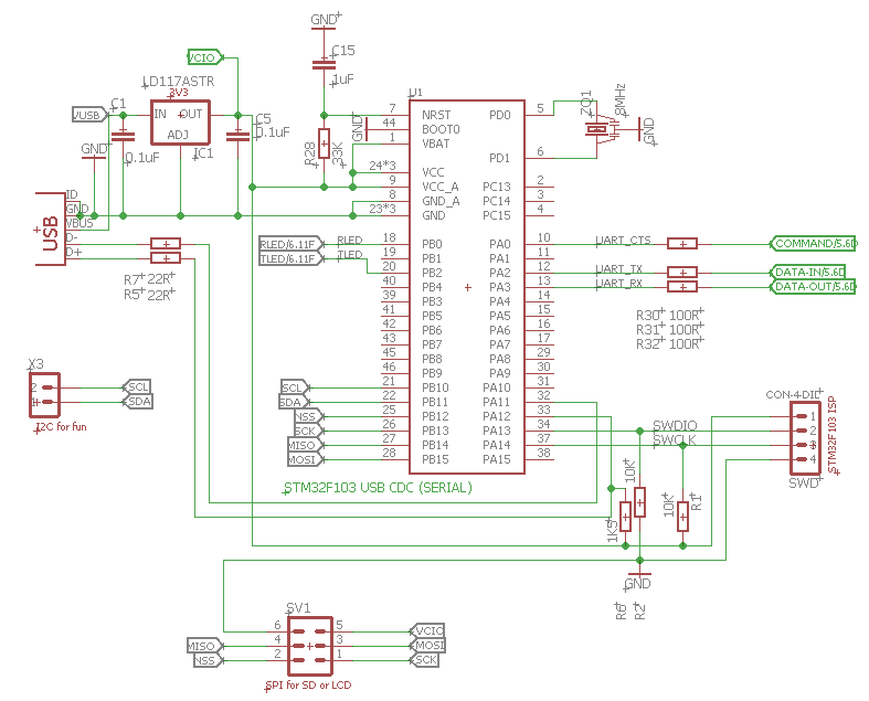
This module is powered from USB. The only important resistor is R6 – 1.5K, other resistors are very tolerant to its value. SWD pull-up/down- 10K…20K, USB line protection (R5,R7) 22R-100R, MCU reset- R28,C15. There is a 5V-3V3 logic connection via R30-R32. About 100R is enough.
The Regulator chip must be 3V3 output, not adjustable. There are large series of chips with 1117 in the name. Connect USB cable to computer- if MCU is empty, computer will report unknown USB device. It will report this error even if MCU is not soldered or bad- the magic of 1.5K resistor.
Now we need to upload firmware to the chip. Buy this thingy:
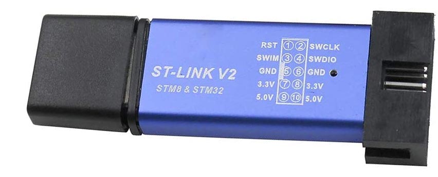
Download drivers, install them and run command line from folder with hex file:
st-link_cli -c SWD -p daigciukas.hex -Rst
Remove firmware upload thingy and USB cable. Connect USB cable again and the computer must report that “ATARI 1088XEL” is connected, but soon, after driver install, there will be just another serial port.
Step 4:
I would like to recommend soldering ALL small RC components first. It is much easier to put them on PCB then there are no big parts nearby. It is possible to use solder paste, heat-gun (IR soldering station) or any other mass soldering tools here. I think it is possible to order pre soldered PCBs from some PCB houses.
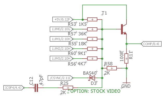
There may be some parts left unsoldered- if you have UAV module, there is no need to solder “stock video” option:
Step 5:
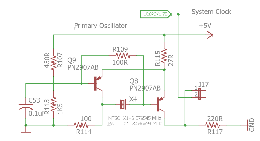
For the stock clock, build this part:
About transistors: I used scrap PNP transistors from some old PCB. Any generic PNP and NPN will work in Atari. I am using very HF transistors [BFR106] only because I have spool of them. All diodes are double BAV99 (in some places only 1/2 is used).
And power the board. If you have an oscilloscope- you can check the first heartbeat of the computer on a J17 jumper.
Solder small SMD logic chips. Possible chip versions are described in the BOM section of this manual.
Always check voltage on the 5V rail- if there is a big drop, or your temporary resistor on L2 is smoking, there must be a big error somewhere. At this moment computer do not use much power at all. Populate chips sockets, cartridge slot (part of old ISA connector), jumper headers, PS/2 connector, audio connector, video connector, variable resistor, electrolytic caps. Power on computer- there must be no power surge, computer stays mainly static. If you have an oscilloscope, check for clock on “System Clock” bus- VGATE pin 2, GTIA pin 28.
Now, take your first Atari chip- GTIA. Power off and put GTIA to socket (in future I will not repeat the mandatory power of while placing and removing chips. Full power cut off, not power button press).
Power computer- now we can check more signals, and even your TV or Video monitor can catch video output (blank screen). If you have an oscilloscope, check GTIA pin 29 for clock (3.5..MHz), same clock on ANTIC pin 35.
Populate ANTIC chip. Now check for the main clock (1.7..MHz) for the CPU. Add CPU (Sally). When adding each Atari chip, take note that power consumption increases, and as we have resistor instead of inductor, voltage on the 5V rail will get lower.
After populating all Atari chips, power consumption must be about 3W.
Step 6:
If you have “U1MB” module, do not solder the MMU socket. Solder two pin headers here for this module. If there are no plans for “U1MB”- solder 20 pin socket for PAL/GAL/PALCE Atari MMU.
Place TK-II PIC chip- it is the only mandatory “hobby” chip for this Atari model. It handles reset circuit and keyboard interface.
In the case “stock” version of Atari 1088XEL SMD the only one missing part is OS ROM. And it is the only chip on the riser PCB.
OS ROM riser is straight pin-to-pin module to some EPROM/EEPROM. I made some riser PCBs for it. The PCB is not only for Atari risers (MMU and ROM), but also for Commodore 64 cartridge and ZX81 video conditioner. Also, some spare space used for Z80 CPU debug board and some 555 timer stuff.
Schematics for add-ons.
TOP View, BOTTOM view.
Gerber files: Some risers, Z80 board, ZX81 video, Atari MMU, Atari OS BASIC ROM. Mill layer is wrong and I am not planing to fix it. Just remove it or redraw- I’ve cut this PCB by hand.
Original version of MMU chip requires that BASIC and OS are on different chips. Original Atari 1088XEL do not use MMU and standard ROM chips. In the case of the “stock” version, the only mandary ROM chip is OS. Basic is option. It is possible to put both OS and BASIC images to same ROM chip, but someone must modify MMU chip. In the 21-st century it is big problem to program GAL/PAL/PALCE chip. For more information about these “basic” PLD/CPLD devices visit the MMU part of this manual.
There is a BASIC jumper on the PCB near the audio connector. This is only for compatibility with the original 1088. In the original computer, one pin of the pin header is connected to +5V, meanwhile I traced “basic enable” net to this pin. I use this pin to change the ROM page and select BASIC ROM. Even with stock MMU and small additional logic it is possible to enable basic. Or just write a basic image to the ROM cartridge.
After placing OS ROM, computer must boot to ROM diagnostics menu, with BASIC ROM – to basic prompt. Computer will attempt to boot from the SIO port, if there is a DISK emulator connected, it will boot from the “disk”. There is no difference in hardware handshaking- all handshaking is the same. Firmware just checks the status of the atari bus and reports to all serial port status pins at same time.
I used two evenings to solder this toy from an empty PCB to a full working computer. But please, do not hurry, have a nice time.