
As I mentioned in previous posts, one company supplied me by few Altera Cyclone II (EP2C5T144C6N) FPGAs. All these chips were soldered to some rejected circuit boards. Board were damaged by improper soldering, mainly by overheating and PCB track unstuck from the base. I selected one board with minimal visual defects. There is place for JTAG connector, so I soldered it, used 3.3V power mentioned in previous post and chip replied on the JTAG chain.
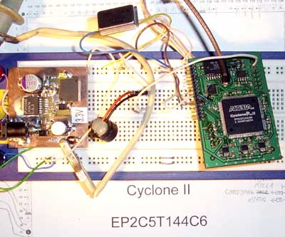
After few experiments and three kynar wires, I manged to set chip in JTAG programming mode and programmed small testing code to it. It is working and I hope that other chips are good too. In Lithuanian version of weblog I described how to set this PCB to jtag mode, but this entry is just for myself. If I’ll need to use other boards, I’ll have detailed instructions. English language reader will not find such PCBs in their local stores.
Thanks to local company for nice set of Cyclones and also, for about twenty Atmel ATMEGA16 chips!
What is Cyclone?
The Cyclone II architecture consists of more than 68K vertically arranged LEs, embedded memory blocks, embedded multipliers, and phase-locked loops (PLLs) that are surrounded by I/O elements (IOEs). A highly efficient interconnect and low-skew clock network provides connectivity between each of these structures for clock and data signals.
Area-efficient IOEs are grouped into I/O banks around the device, offering significant capabilities while consuming minimal die area. Cyclone II devices support a wide range of single-ended and differential I/O standards, such as the LVDS I/O standard at up to 805 Mbps (receive) and 622 Mbps (transmit). Each IOE contains three registers for implementing DDR applications and associated circuitry for other I/O features such as programmable drive strength, bus hold, and programmable slew rate.
Several I/O banks are equipped with dedicated external memory interface circuitry. This circuitry simplifies data transfer with external memory devices, including DDR2 and QDRII SDRAM devices. Maximum data transfer rates reach speeds of up to 333 Mbps (167-MHz clock).
Cyclone II devices implement the same embedded memory blocks available in the original Cyclone family. The Cyclone II family includes up to 250 embedded memory blocks, which are ideal for use as program storage memory for embedded processors or header or cell storage.
Cyclone II devices are PCI revision 2.1 and PCI-X revision 1.0b (Rev 2.0 mode 1) compliant. Each IOE provides multiple paths from the pin to the core, allowing the device to meet associated set-up and hold times.
Cyclone II devices range in density from 4,608 LEs and 119,808 bits of RAM to 68,416 LEs and 1,152,000 bits of RAM. From 13 to 150 18 x 18 embedded multipliers are available within Cyclone II devices.
Advert:
