This is simple, quite powerful and economical power supply. You don’t need to switch it off- when load is off, the psu draws on fraction of Wat of the power. (80 mW @ 110 VAC, 160 mW @ 230 VAC). The main component is TOP242-250 chip.
Special transformer is used in this supply.

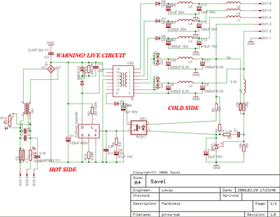
Schematics for printing and viewing.
The schematics is universal. It is possible to change output voltage and number of outputs. Also it is possible to change the power of whole power supply. When using most weak chip in closed box without ventilation, it is possible to build 10W power brick. Using most powerful chip and proper cooling- the power increases up to 290W!
The schematics consist of few main modules:
Live side rectifier and filter. It is used to produce high voltage DC and to filter all possible interferences.
Strange resistor near C18 is NTC resistor. It is used to reduce current spike when device is plugged into mains. C18, TR1, CX and C3 are used to filter all high frequency stuff from and to the device. If device is made in Chinese way, all this stuff can be omitted. R12 (the symbol in circuit diagram is bad) is varistor. It is used to protect the device from voltage surge. If voltage is more than 270V it shortens the mains and fuse blows. We can add R2 to the protection circuit. When voltage in DC side is more than some value defined by R2, the top switch chip is switched off.

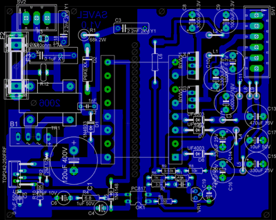
As you can see from PCB image, some duplicated devices (like F2 and F3, CX1 and CX2) are place on on others top. This makes PCB more universal- it is possible to use different size devices. Additional chokes (L6-L9) are just simple jumpers. It is possible to make PCB without them, but some traces will become much narrower and longer. And this PCB is designed to be with thick tracks. So everybody can make it using all simple PCB making technologies.

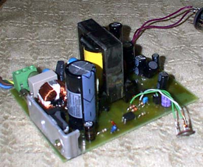
Side view of the PSU. That trimmer is used to adjust output voltage. When PSU will be tuned, the trimmer will be replace with simple resistors.
