Now let’s speak about the pins.
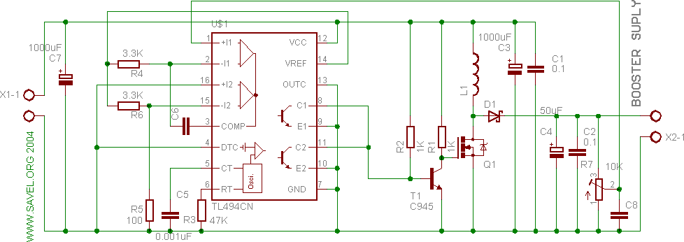
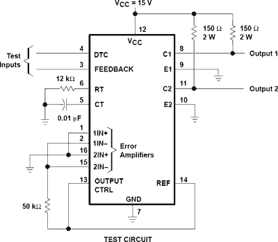
GND (pin 7) and Vcc (pin 12) are usual power pins. Max Vcc is about 40V.
RT (pin 6) and CT (pin 5) are used for setting clock (1 … 300kHz). The frequency of the clock is calculated using table from data sheet and changing resistor (1.8 … 500 kΩ) and capacitor (0.47 … 10000nF). Or the on-chip oscillator can be bypassed by terminating RT to the reference output and providing a sawtooth input to CT, or it can drive the common circuits in synchronous multiple-rail power supplies.
REF (pin 14) is 5V reference output. Low power output- 10mA.
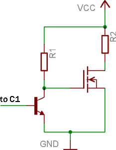
Pin FEEDBACK (pin 3) is used to control the pulse width. Is the input is zero, the width is maximum, if it is ~5V or more (compared to REF) than output is disabled. Input must be less than Vcc.
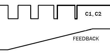
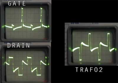
Output vs Feedback
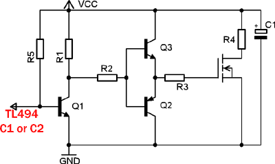
DTC (pin 4) is Dead Time Control. This pin is similar to feedback, but it is used to make soft start. Regardless to FEEDBACK it controls the width of the pulse. If it is more than REF (~5V) the output is disabled, if zero- output is maximum and controlled by FEEDBACK. Here is example:
Simple soft start
There is small difference in DTC and FEEDBACK. It can be understood by reading data sheet.
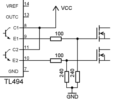
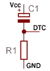
C1 (pin 8 ) is collector of output transistor #1.
E1 (pin 9) is emitter of output transistor #1.
C2 (pin 11) and E2 (pin 10) are like C1 and E1, but for the transistor #2.
The output is max 200mA on each transistor.
OUTPUT CTRL (pin 13) is setting the type of output. If it is high (=REF), the output is two phase. If input is GND, the output transistors are working in same phase, so you can can connect them in parallel and thus, get more output current.
The last pins are used in error control unit. They are used to detect various errors and make protections from short circuit and under-, over-voltage protection. I’ll describe them in the other post.
Next tutorial lesson.