
I have Sinclair QL, “issue 5” with 3 EPROM chips. One of the chips is riding on the other chip. And yes, it is the original solution from Sinclair engineers- they were pressed by Apple computers new product and they had to make it fast. This computer had some problems- the screen was filled with garbage and nothing was working. Looks like a RAM issue, but original firmware is not very good at diagnostics. It is very nice that there is a third party ROM for this computer and it is possible to download ROM image. This ROM image will not fit to single ROM in current configuration and it is quite crazy to piggyback ROM chips. This topic is also commercialized in retrocomputer world, but there is very simple fix.
First, I just placed a small PCB to test the computer and check RAM. The RAM was good, problems were in piggyback ROM.
(Some images are clickable)
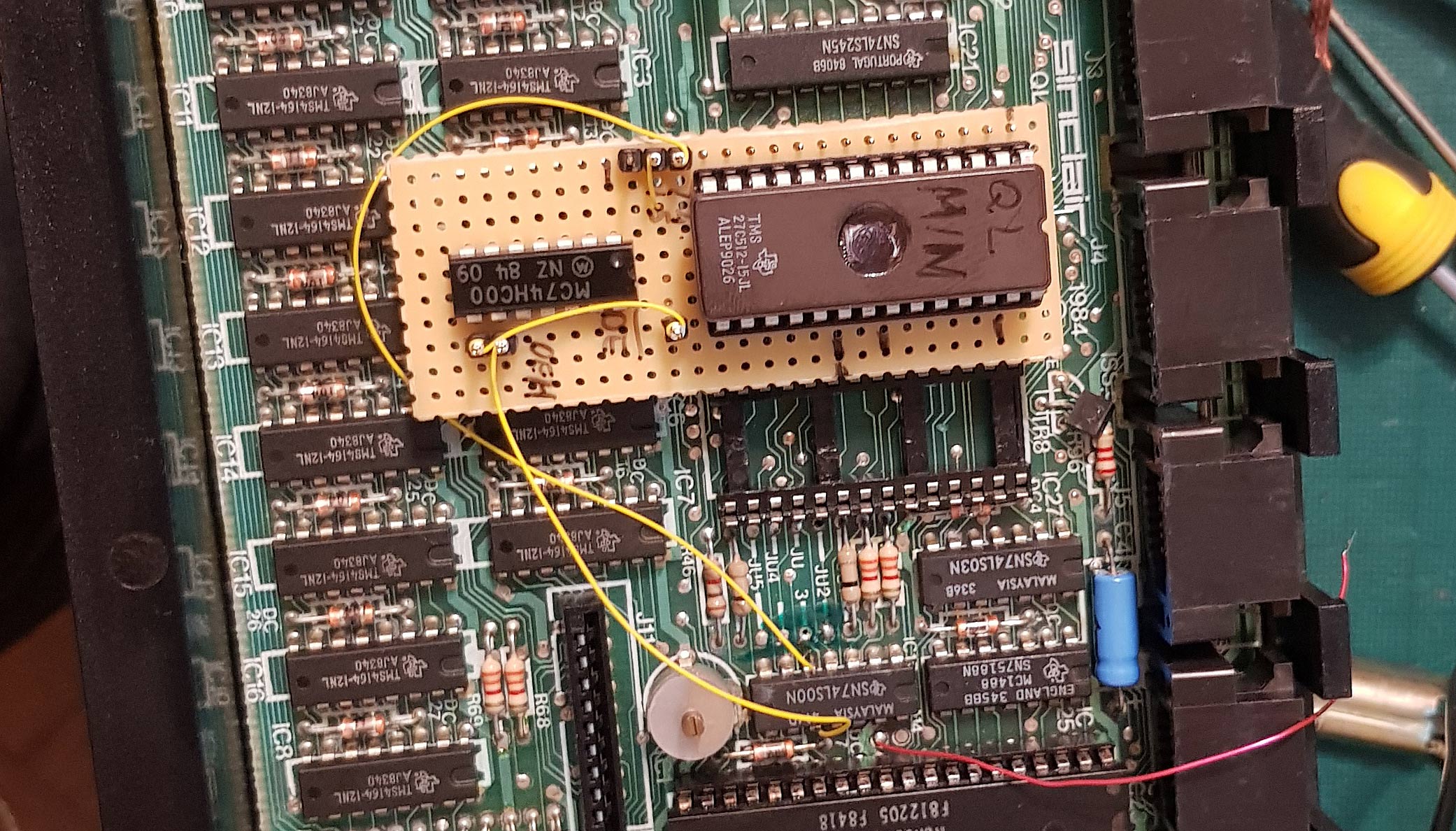
Computer requests ROM’s chip select rising HIGH ROM_OEH. Typical EPROM chips use inverted CS/OE pin. So, I placed a 74HC00 chip to invert the signal. And one wire for the missing address pin.
After power on, I have the image:
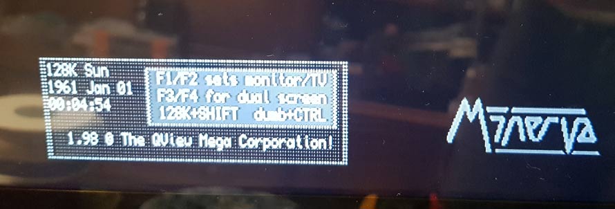
(No colors because I do not have the original multi voltage PSU. Computer is powered from 5V rail only, so no PAL output and no RS232. Yes, it runs from 5V only.)
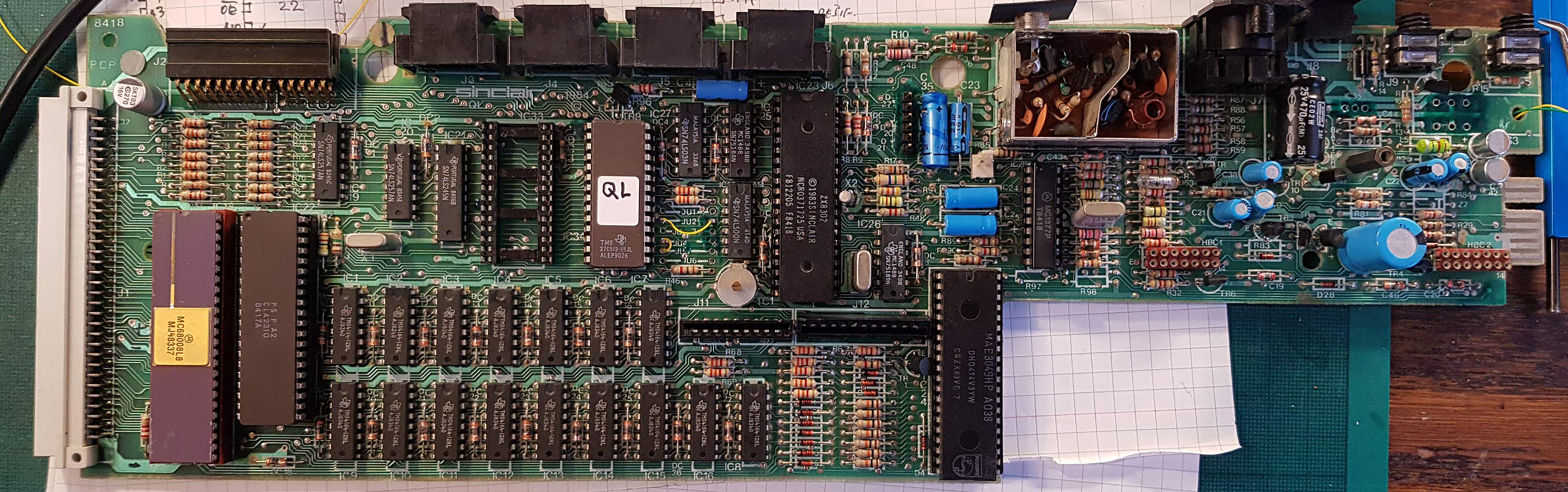
Now time to make it beautiful and remove all alien PCBs. This model QL (issue 5) is using standard EPROM instead of MASK ROMs and OE signal inversion and some sort of address decoding is done with 74LS00 chip on board. Models with MASK ROM have this chip removed or unpopulated at factory. We will use this useless chip for ROM_OEH inversion. I removed all jumpers on ROM decoding circuit and cut several ones (detailed information is below) and there is final result:
Now about the modifications:
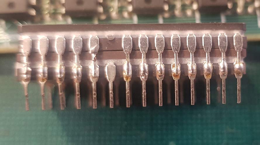
Original or third party ROM image can fit to a 27C512 chip, also, this chip can fit to one of original sockets for ROM. But there must be several modifications done. The PCB was designed without knowing that in near future there will be bigger chips, so A15 pin is very very hardwired to Vcc. To cut out this pin, I removed ROM socket, cut around this pin and soldered the socket back. Meanwhile, the original A15 signal is connected to CE of both ROM sockets. Cut A15 from this pin and connect CE to ground.
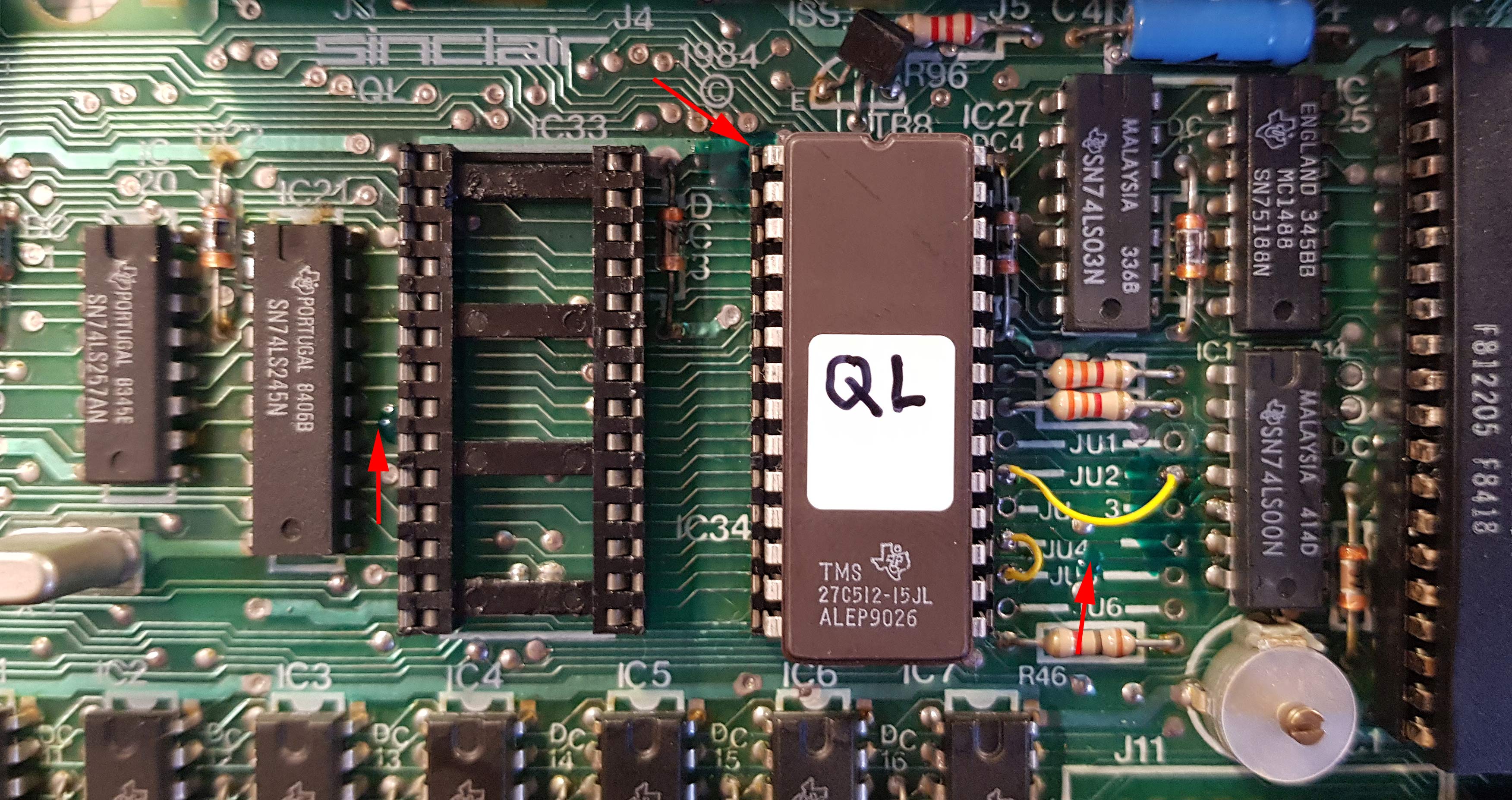
In this foto, red arrows show cut lines. And only two yellow short wires are jumpering all needed connections on this side of PCB. Press on image for better view. I isolated the cut line with green UV curable PCB mask paint.
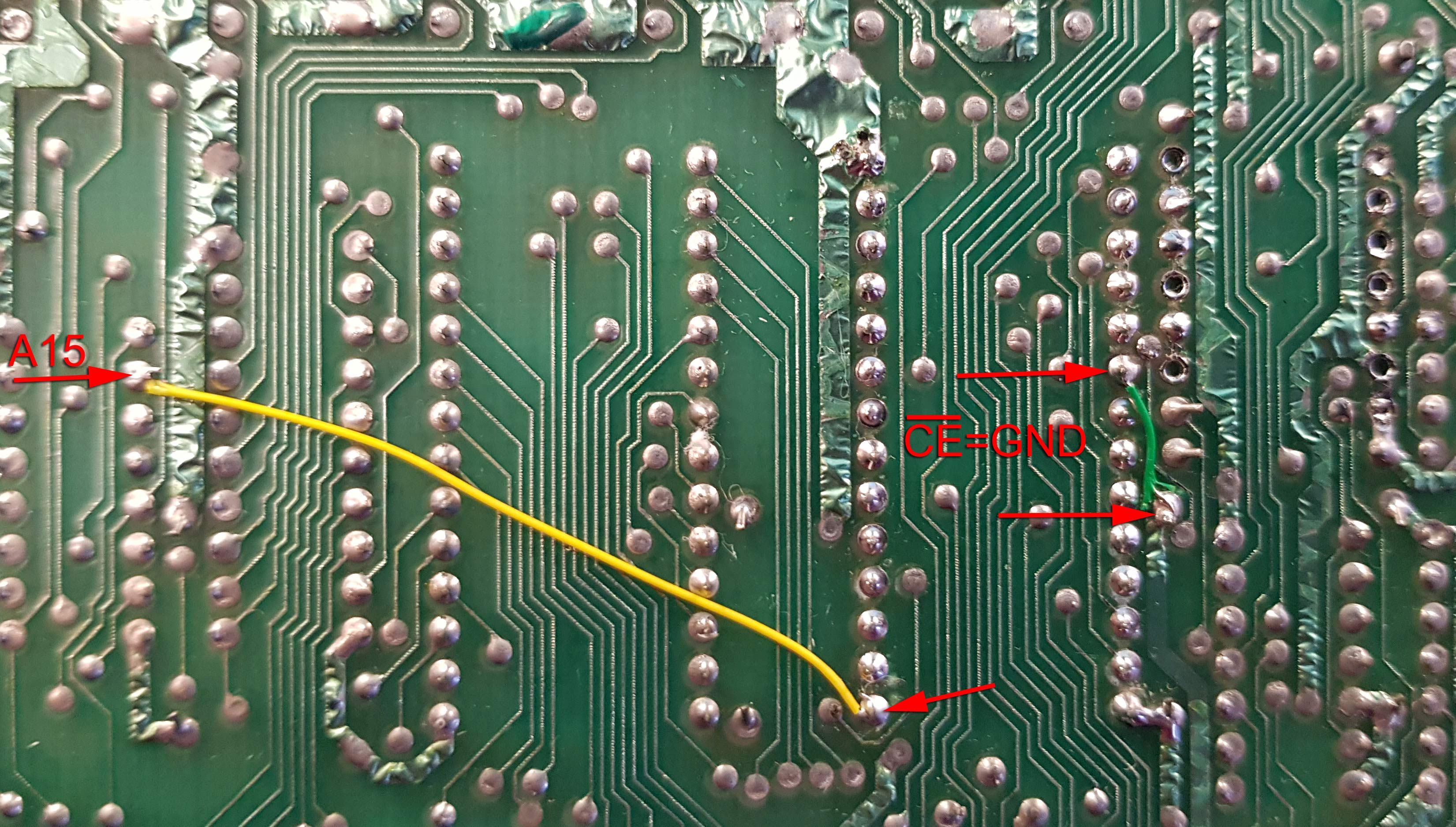
The back side (solder side) of the PCB. There are two jumper wires here. Green on is connecting GND to CE pins of the ROM socket, long yellow wire is for A15 signal. I cut it too far from the chip, but it is still a very nice connection.
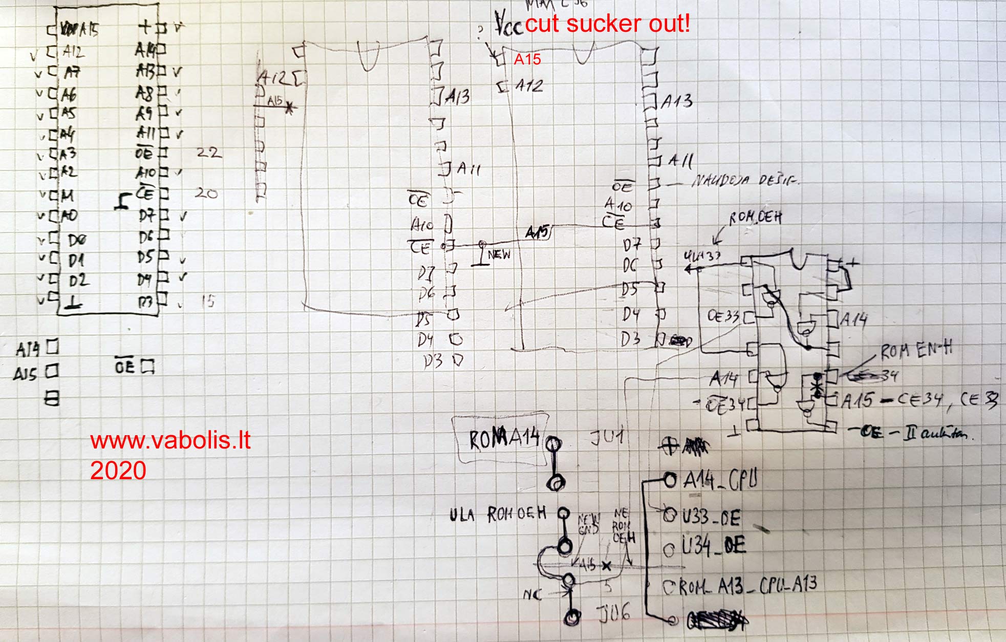
All these modifications were done using only original schematics and here is a photo of my sketched chicken schematics. Sorry for dual handwriting, I am ambidextrous, but my “font” is different in left and right hand.