
Just short story about my experiments using CPLD chip and Lattice software.
I forced myself to use and learn about programmable logic chips. As I wrote in my older post, I have very small inventory of the chips and was forced to use Lattice isp2032VE110LT144 chip. I received great help reading article from Seattle Robotics Society web page. Also, at same time I was experimenting with controller-less LCD screen module. So I joined both ideas to one project and here is the result.
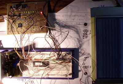
Also in this project is used my universal dual output power supply from older post.
The theory about LCD control was tested using big computer and MS Visual Basic software. CPLD programing software I downloaded from Lattice Semiconductors site. The chip was soldered to self-made testing PCB.
And now few words about programing of the CPLD devices…
I started ispLever Navigator and started my project from nill. I not too smart to wrote all signals is HDL (hardware description language) so I selected mixed type of the project: ABEL + Schematics. So I can describe some modules in ABEL language and connect all modules using graphics editor in schematics editor. I selected ABEL as I had some examples already written in it.
In theory I need to feed LCD with clock, vsync and hsync pulses. It is very easy to describe column and row detection logic modules. Here is row detector (eiles.abv)
MODULE eilutes

TITLE 'Eiluciu skaitiklis'

declarations

 a8..a15 pin;

 out pin istype 'com';

 adresas=[a15..a8];

equations

 out = (adresas == 208);

END
In ABLEL language there are few mandatory fields: MODULE – name of the module; declarations- declaration of the variables and wires; equations- the logic formulas itself. In this example we use whole bunch of wires or bus called a[] – a8, a9, a10 and etc. up to a15. I collected wires to bus for easy description. In equations section we just test the bus for some value. The column detect is identical (stulpai.abv):
MODULE stulpeliai

TITLE 'Stulpeliu skaitiklio dekoderis'

declarations

a0..a7 pin;

out pin istype 'com';

adresas=[a7..a0];

equations

out= (adresas == 160);

END
The binary counter is a bit more complicated. I use two types of counters in this project- one is 4 bit counter for dividing frequency of master clock (count4.abl):
MODULE skaitliukas4

INTERFACE (clk ->q3, q2, q1, q0);

TITLE 'skaitliukas 4 bitai'

DECLARATIONS

    clk      pin ;                "Clock input

    q3..q0   pin istype 'reg';    "Counter outputs

    count = [q3..q0];             "Creating output bus

EQUATIONS

    count.clk = clk;              "Counter clock input

    count := count + 1;

END
This counter is created using example. I only simplified it. It just divides the master clock. Other counter is more complicated- it has reset pin (count8.abl):
MODULE skaitliukas8

INTERFACE (clk, rst -> q7, q6, q5, q4, q3, q2, q1, q0);

TITLE 'skaitliukas 8 bitai'

DECLARATIONS

    clk      pin ;                "Clock input

    rst      pin ;                "Asynchronous reset

    q7..q0   pin istype 'reg';    "Counter outputs

    count = [q7..q0];             "Creating output bus

EQUATIONS

    count.clk = clk;              "Counter clock input

    count.ar  = rst;              "Counter reset input

    count := count + 1;       "Counting when ld low

END
IspLever software generate schematic symbols from these scripts and they can be placed into circuit diagram as components. So I added some standard logic and here is the result:
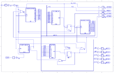
(Big circuit diagram for printing)
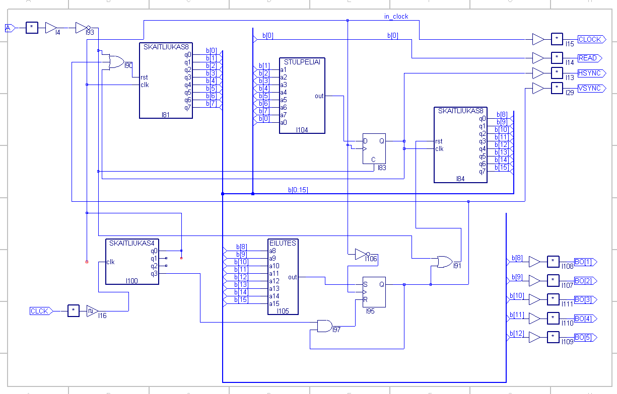
It is possible to simulate and test the circuit just using software in your computer. There is special software for this and you can watch all oscillograms on the screen. The problem is, that to test all LCD logic the computer must simulated whole screen timings- tens of thousands of clock tics. It took lots of memory and time in computer. You must have quick one.
Now we can star “Constraint Editor” and connect all signals to real pins of the chip. It is possible to describe pins in ABEL language, but is much easier to do it in graphic interface. And it much more easier to change the pins in visual way.
Now start “LSC ispVM System” program and program real chip using JTAG cable. And now time for experiments and fine tuning of the project- just change, recompile and reprogram the chip. The chip can be reprogrammed tens of thousands times, so don’t worry. 🙂
In the image you can see part of the LCD screen with chaotic image. This image is generated from ROM chip- it is used as “video RAM”. But the project is closed as the chip is too small for this project. Maybe I’ll finish this project using FPGA chip.
Thanks for a detailed description about using CPLD & good luck with future experiments.
Dave