
Some introducing to programmable logic chips or just my throes…
I was forced to learn about programmable logic. The mental outfit is zero. I only know that there are such devices.
The most simple and oldest CPLD (complex programmable logic devices) are PAL (PALCE) and GAL chips. The problem is, that you need special programmer to program these devices. There is ONE (!) (galblaster) circuit diagram in the whole internet for GAL chips. It is old, maybe buggy and quite complicated device. Software is designed for old OS and maybe not running on modern, fast computer, running in hardware protected mode. And NONE (!) for PAL and electrically erasable PALCE chips.
So I take a glance to next generations chips. They are programmed using serial JTAG (or similar) interface and can be reprogrammed for many times. You even don’t need to pull out the chip as it is programmed in in circuit programmed mode (ISP). No need for complicated programming devices, the software is available from manufacturer for free. The flip-side of these chips- they are expensive and rare to find in Lithuania. The current support for hobbyist in Lithuania is awful. The only way to get device is to order by mail, buy in ebay or salvage from old equipment.
I selected last way to obtain the devices. The only source is the old electronic devices. But these devices must be rare, not used in wide market. It must be some communication equipment, some scientific devices, custom design computers and peripherals and other stuff. You must have luck and good eye to spot chip in junk pile.
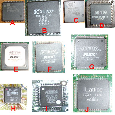
Here is my booty:
(I have some more ALTERA devices, but with BGA package. This package is still not usable by my technology.)
A and C is AMD Mach 110 and 120 series chip- I don’t have software.
B- Xilinx FPGA XC3142A, current demo software didn’t support it.
D- Altera EPM7032LC44-15T – untested, but it seams not supported by current software.
E, F, G – Altera’s FPGA Flex line (EPF10K10TC144, EPF81188ARC240, EPF8636AQC208) – only one chip supported by software.
H- Lattice isp2032VE110LT44 – Fully supported by software.
I- EPM3032ATC44 – supported by software, but the chip is in working device.
J- Lattice ispLSI2128 100LT- software supports chip with “A” in the part number. Datasheet describes “A” as enhanced version of plain chip, but software is not supporting this device id. It even didn’t scan JTAG chain, but the device is working (or problems in current PCB). I need this chip working.
You need special software to compile the chip “design”. The software produce jedec file. This filed is programmed to device using any programmer. Typically you can find software in chip manufacturer’s site. The problem is, that software is very expensive. The demo version is supporting only few, “promotional”, devices. This factor reduce my selection.
FPGA (field programmable gate array) devices are very cool, but the configuration is stored in static RAM, so after power down, the configuration is lost and the device must be reprogrammed again. This is done by special small ROM chip, some MCU or using JTAG cable and “big” computer. For my first experiments I would like to use less complicated programming. So I selected CPLD with build in flash memory.
Another important fact is package. As I mentioned above, I can’t use BGA. Other chips with hundreds of tiny pins are not very suitable for me. I must select “older” devices with thick pins or new devices with small pin count.
So the only chip for my first further acquaintance is Lattice isp2032VE110LT44.
• SuperFAST HIGH DENSITY IN-SYSTEM
PROGRAMMABLE LOGIC
— 1000 PLD Gates
— 32 I/O Pins, Two Dedicated Inputs
— 32 Registers
— High Speed Global Interconnect
— Wide Input Gating for Fast Counters, State
Machines, Address Decoders, etc.
— Small Logic Block Size for Random Logic
— 100% Functional, JEDEC and Pinout Compatible
with ispLSI 2032V Devices
• 3.3V LOW VOLTAGE 2032 ARCHITECTURE
— Interfaces With Standard 5V TTL Devices
• HIGH PERFORMANCE E2CMOS® TECHNOLOGY
— fmax = 300 MHz Maximum Operating Frequency
— tpd = 3.0 ns Propagation Delay
— Electrically Erasable and Reprogrammable