
Everything is working with simple passive mosfet drive. But if we increase switching frequency or place powerful mosfet (or even several mosfets)? There is no load in gate circuit, but there is gate capacitance. And if we need fast switching we must charge and discharge gate very quickly. With passive drive there are limitations. We can use active charge-discharge circuit. Also this circuit uses inverter transistor for proper signaling:
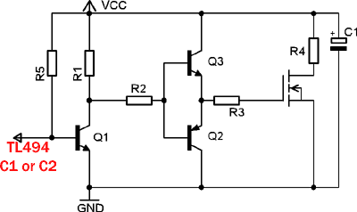
Totem pole mosfet drive (push-pull)
Few comments about schematics. R5 is TL494 output load- anything about 1K. R1 is Q1 load, not critical- 1K. Q1 inverts signal from controller. R2 is used to prevent overload of totem pole bases. Q2 and Q3 are complementary pair. R3 are useful if are few mosfets on the output, only few ohms. Q1 and Q3- C945, Q3-A733. All transistors from old PC power supply. R4 – load simulation.
(C945- npn transistor, ~50V, 100mA, 200mW; A733- pnp, ~50V, 100mA, 200mW)
Connect pair of these totem poles and connect to transformer like in older post. You can notice small increase of the performance. Don’t overload. There are lots of parasitic oscillations in this circuit.
Pingback: Savel brain dump in English! » Blog Archive » TL494 - magic chip, Part 4
Googled in following MOSFET driver image, *finally* thought to put the …829a in your blog’s search-box.
Couldn’t find what Vcc was in *this* circuit, but I’ll re-work generic values for 12 Volts ( Lead-acid 10–15 😉 anyway…
Hmm: I’d add a 5v6 zener Gate / Source, but I’m paranoid.
“May The Magic Smoke Remain In Your Circuits !!”
Nik
These schematic dos not work, why because R1 activate Q3 so mosfet is fully ON hotttttt. Just remove R1, R5, Q1, and R2. Connect directly to pin 9&10 and pin 9, 10 need resistor 3.9K to ground. Work nice trust me I spend to much time with this.
Schematics are working and fully tested.
I desagree with Jef because you should take into account that Q1’s base is kept low because of 494 Cx output is active low, so Q1 is normally active => R2 is connected to ground, leaving the MOSfet off
Jeff is an asshole……..
R2 is an ass hole.
i have built the circuit and have a great pulse on both c1 and c2 but when i connect this driver circuit i have no pulse at the gate of the mosfet. i have checked all connections about 40 times and they are accurate to your schematic here. any ideas???
forgot to mention power feed to the circuit is between 10-15v
michael: c1 and c2 are colector of q1 and q2? The circuilt is quite simple and consist of two stages: first- signal inverter on q1. Next stage is totem pole driver. Note, that transistors are different npn and pnp. It is so called complementary pair transistors. As structure is different, one transistor is opened while other is closed. R2 limits base current, if it is too much high your transitors will be dead.
You must find pulses on emiters of Q2 and Q3.
If you mean by C1 and C2 that it is output of TL494? Check if your load resistor R5 is in proper value (1…2k for 15V). Also, try to add base current limited resistors (not in the circuit image). They act like R3 and are about few hundreds ohms or few k.
Check your Q1, it may be dead because of high eb voltage. In my experiments I was not using 15V and many transistors have low max Ueb. Either limit voltage or use resistors to divide output voltage.
BTW, transistor may be half-dead 🙂
Check this image: http://www.vabolis.lt/stuff/20090913a.gif, as you can see, output voltage is from Uref (only 5V)
It is part of quite good workbench PSU, sorry, not translated to English:http://www.vabolis.lt/2009/09/13/reguliuojamas-maitinimo-saltinis-nuo-5-iki-100v/.
i decided to use a dual high speed mosfet driver IC triggered off of pins 9 and 10. not my circuit works perfect with strong gate drive signal. thanks for your tutorial
An old post, but this may still be useful; due to output of tl494 C pins being transistor collectors, they don’t go all the way to 0V, rather 0.6-0.7V , this can result in the transistor Q1 always conducting , depending on exact transistor and make of TL494. It can also result in the transistor Q1 switching off, but not at the correct time, leading to a shortened maximum on time of the FETs.
I think due to output of tl494 C pins being transistor collectors, they don’t go all the way to 0V, rather 0.6-0.7V , this can result in the transistor Q1 always conducting , depending on exact transistor and make of TL494. It can also result in the transistor Q1 switching off, but not at the correct time, leading to a shortened maximum on time of the FETs.
Dear admin, great tour and I love this!
In page 3, you said it’s passive mode and it’s not good enough; in part5, you said it’s active mode it’s good. But I can’t understand this, what’s the difference between these two designs?
In page 3, the gate either connected to VCC or to ground through the transistor, so it can fast charge and discharge; While in page5, the gate is either connected to VCC or to ground through q3 and q2 as well. not much big difference ? or, is it because R1 in page2 design? R1 make it not efficient enough?
thank you!
Sorry, it is very old post. Passive mode is good for slow design where is not problems with switching loss. If using bigger capacitance loads and 21st century switching speeds, passive mode is too slow to discharge mosfet/igbt devices.
For 21st century I would recommend to use modern device to drive output or even all in one device.
The difference in connection give different phase of opening and closing devices. When connecting load in emiter side, the phase is the same, when connected in colector side- the phase is inverted.
i have charger used tl494 i want 1- always run , ( non stop ) what could do in ic
and 2- if i want more current ( full current ) ?
thanks